- 您现在的位置:买卖IC网 > Sheet目录872 > P024T048T12AL (Vicor Corporation)V.I CHIP PRM REGULATOR 48V 120W
�� �
�
�Pin� /� Control� Functions�
�+In� /� -In� DC� Voltage� Ports�
�V?I� Chip� Regulator�
�The� V?I� Chip� maximum� input� voltage� should� not� be� exceeded.� PRMs�
�have� internal� over� /� undervoltage� lockout� functions� that� pr� event�
�AL� Version�
�VH�
�SC�
�A�
�B�
�4�
�3�
�2�
�1�
�A�
�B�
�VC�
�PC�
�operation� outside� of� the� specified� input� range.� PRMs� will� tur� n� on� when�
�the� input� voltage� rises� above� its� undervoltage� lockout.� If� the� input�
�voltage� exceeds� the� overvoltage� lockout,� PRMs� will� shut� down� until� the�
�overvoltage� fault� clears.� PC� will� toggle� indicating� an� out� of� bounds�
�condition.�
�+OUT�
�SG�
�OS�
�NC�
�CD�
�C�
�D�
�E�
�F�
�G�
�H�
�J�
�C�
�D�
�E�
�F�
�G�
�H�
�J�
�TM�
�IL�
�NC�
�PR�
�+IN�
�K�
�K�
�+Out� /� -Out� Factorized� Voltage� Output� Ports�
�These� ports� provide� the� Factorized� Bus� voltage� output.� The� –Out� port� is�
�–OUT�
�L�
�M�
�N�
�P�
�L�
�M�
�N�
�P�
�–IN�
�connected� internally� to� the� –In� port� through� a� current� sense� resistor.�
�The� PRM� has� a� maximum� power� and� a� maximum� curr� ent� rating� and� is�
�Bottom� View�
�protected� if� either� rating� is� exceeded.� Do� not� short� –Out� to� –In.�
�VC� –� VTM� Control�
�The� VTM� Control� (VC)� port� supplies� an� initial� V� CC� voltage� to�
�downstream� VTMs,� enabling� the� VTMs� and� synchronizing� the� rise� of�
�the� VTM� output� voltage� to� that� of� the� PRM.� The� VC� port� also� pr� ovides�
�feedback� to� the� PRM� to� compensate� for� voltage� dr� op� due� to� the� VTM�
�output� resistance.� The� PRM’s� VC� port� should� be� connected� to� the� VTM�
�VC� port.� A� PRM� VC� port� can� drive� a� maximum� of� two� (2)� VTM� VC� ports.�
�PC� –� Primary� Control�
�The� PRM� voltage� output� is� enabled� when� the� PC� pin� is� open� cir� cuit�
�(floating).� To� disable� the� PRM� output� voltage,� the� PC� pin� is� pulled� low� .�
�Open� collector� optocouplers,� transistors,� or� relays� can� be� used� to�
�control� the� PC� pin.� When� using� multiple� PRMs� in� a� high� power� array� ,�
�the� PC� ports� must� be� tied� together� to� synchr� onize� their� turn� on.�
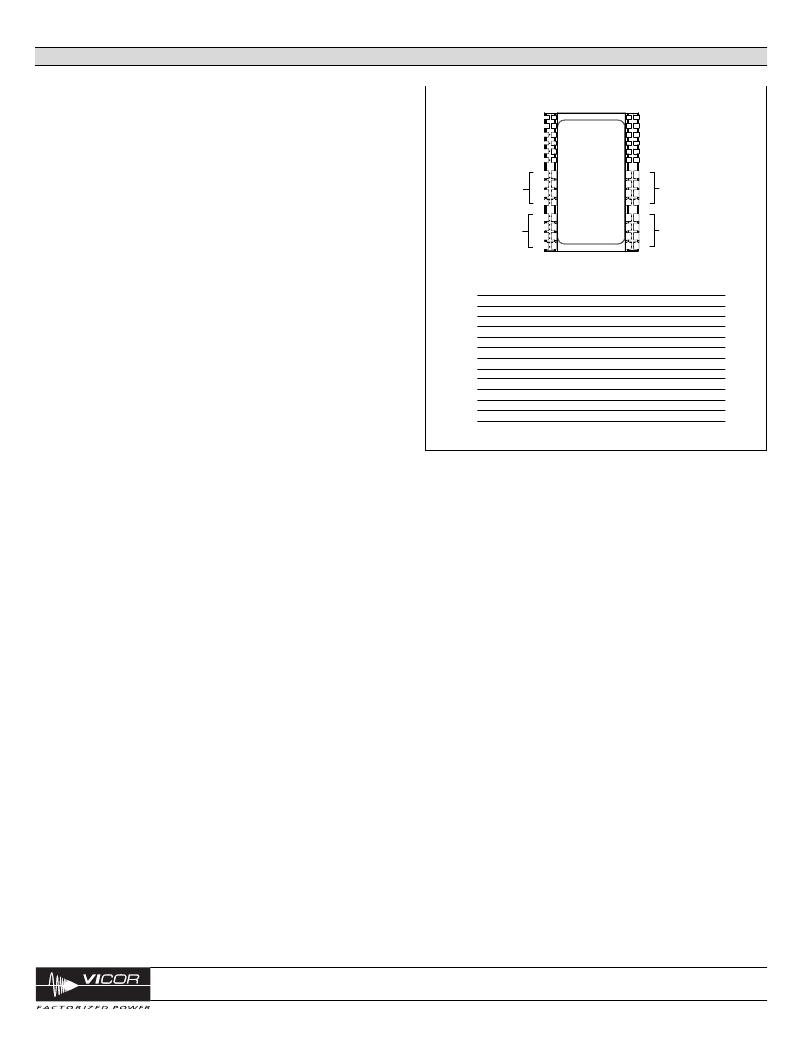
�Signal� Name�
�+In�
�–In�
�VC�
�PC�
�TM�
�IL�
�PR�
�VH�
�SC�
�SG�
�OS�
�CD�
�+Out�
�–Out�
�Figure� 15� —� PRM� pin� configuration�
�Designation�
�G1-K1,G2-K2�
�L1-P1,� L2-P2�
�A1,A2�
�B1,� B2�
�C1,� C2�
�D1,� D2�
�F1,� F2�
�A3,� A4�
�B3,� B4�
�C3,� C4�
�D3,� D4�
�F3,� F4�
�G3-K3,� G4-K4�
�L3-P3,� L4-P4�
�During� an� abnormal� condition� the� PC� pin� will� pulse� (Fig.12)� as� the� PRM�
�initiates� a� restart� cycle.� This� will� continue� until� the� abnormal� condition�
�is� rectified.� The� PC� should� not� be� used� as� an� auxiliary� voltage� supply� ,�
�nor� should� it� be� switched� at� a� rate� gr� eater� than� 1� Hz.�
�SC� –� Secondary� Control�
�The� load� voltage� may� be� controlled� by� connecting� a� resistor� or� voltage�
�source� to� the� SC� port� referenced� to� SG.� The� slew� rate� of� the� output�
�voltage� may� be� controlled� by� controlling� the� rate-of-rise� of� the� voltage�
�at� the� SC� port� (e.g.,� to� limit� inrush� curr� ent� into� a� capacitive� load).�
�TM� –� Factory� Use� Only�
�SG� –� Signal� Ground�
�IL� –� Current� Limit� Adjust�
�The� PRM� has� a� preset,� maximum,� current� limit� set� point.� The� IL� port�
�may� be� used� to� reduce� the� current� limit� set� point� to� a� lower� value.� See�
�“Adjusting� Current� Limits”� on� page� 10.�
�PR� –� Parallel� Port�
�The� PR� port� signal,� which� is� pr� oportional� to� the� PRM� output� power,�
�supports� current� sharing� of� two� PRMs.� To� enable� current� sharing,�
�PR� ports� should� be� interconnected.� Steps� should� be� taken� to� minimize�
�coupling� noise� into� the� interconnecting� bus.� Terminate� this� port� with� a�
�10� k� equivalent� resistance� to� SG,� e.g.� 10� k� for� a� single� PRM,� 20� k� each�
�for� 2� PRMs� in� parallel,� 30� k� each� for� 3� PRMs� in� parallel� etc..� Please�
�consult� Vicor� Applications� Engineering� regarding� additional�
�considerations� when� paralleling� more� than� two� PRMs.�
�VH� –� Auxiliary� Voltage�
�VH� is� a� gated� (e.g.� mirrors� PC),� non-isolated,� nominally� 9� Volt,�
�regulated� DC� voltage� (see� “Auxiliary� Pins”� specifications,� on� Page� 7)�
�that� is� referenced� to� SG.� VH� may� be� used� to� power� exter� nal� circuitry�
�having� a� total� current� consumption� of� no� more� than� 5� mA� under� either�
�transient� or� steady� state� conditons� including� tur� n-on.�
�This� port� provides� a� low� inductance� Kelvin� connection� to� –In� and�
�should� be� used� as� reference� for� the� OS,� CD,� SC,VH� and� IL� ports.�
�OS� –� Output� Set�
�The� application-specific� value� of� the� Factorized� Bus� voltage� (Vf)� is� set�
�by� connecting� a� resistor� between� OS� and� SG.� Resistor� value� selection� is�
�shown� in� Table� 1� on� Page� 2,� and� described� on� Page� 9.� If� no� r� esistor� is�
�connected,� the� PRM� output� will� be� appr� oximately� one� volt.� If� set�
�resistor� is� not� collocated� with� the� PRM,� a� local� bypass� capacitor� of�
�~200� pF� may� be� required.�
�CD� –� Compensation� Device�
�Adaptive� Loop� control� is� configured� by� connecting� an� exter� nal� resistor�
�between� the� CD� port� and� SG.� Selection� of� an� appr� opriate� resistor� value�
�(see� Equation� 2� on� Page� 9� and� Table� 1� on� Page� 2)� configures� the� PRM�
�to� compensate� for� voltage� drops� in� the� equivalent� output� resistance� of�
�the� VTM� and� the� PRM-VTM� distribution� bus.� If� no� r� esistor� is� connected�
�to� CD,� the� PRM� will� be� in� Local� Loop� mode� and� will� r� egulate� the�
�+Out� /� –Out� voltage� to� a� fixed� value.�
�vicorpower.com�
�800-735-6200�
�V?I� Chip� Regulator�
�P024F048T12AL�
�Rev.� 3.1�
�Page� 8� of� 14�
�发布紧急采购,3分钟左右您将得到回复。
相关PDF资料
P036T048T12AL
V.I CHIP PRM REGULATOR 48V 120W
P045T048T17AL
V.I CHIP PRM REGULATOR 48V 170W
P045T048T32AL
V.I CHIP PRM REGULATOR 48V 320W
P048T048M24AL
V.I CHIP PRM REGULATOR 48V 240W
P048T048T12AL
V.I CHIP PRM REGULATOR 48V 120W
P081N-271F2CBR10K
POT MODULE 8MM 10K SIDE ADJ
P090L-02T20BR50K
POT ROTARY 50K OHM 9MM SNAPIN
P092N-QC15AR20K
POT ROTARY 20K OHM 9MM
相关代理商/技术参数
P0250
制造商:TE Connectivity 功能描述:
P0250.102NL
功能描述:1μH Unshielded Wirewound Inductor 8.6A 9 mOhm Max Nonstandard 制造商:pulse electronics corporation 系列:P0250NL 包装:托盘 零件状态:有效 类型:绕线 材料 - 磁芯:- 电感:1μH 容差:±15% 额定电流:8.6A 电流 - 饱和值:20A 屏蔽:无屏蔽 DC 电阻(DCR):9 毫欧最大 不同频率时的 Q 值:- 频率 - 自谐振:- 等级:- 工作温度:-40°C ~ 130°C 频率 - 测试:100kHz 安装类型:表面贴装 封装/外壳:非标准 大小/尺寸:0.733" 长 x 0.596" 宽(18.62mm x 15.14mm) 高度 - 安装(最大值):0.290"(7.36mm) 标准包装:60
P0250.102NLT
功能描述:固定电感器 1.0uH 15% 20A RoHS:否 制造商:AVX 电感:10 uH 容差:20 % 最大直流电流:1 A 最大直流电阻:0.075 Ohms 工作温度范围:- 40 C to + 85 C 自谐振频率:38 MHz Q 最小值:40 尺寸:4.45 mm W x 6.6 mm L x 2.92 mm H 屏蔽:Shielded 端接类型:SMD/SMT 封装 / 箱体:6.6 mm x 4.45 mm
P0250.102T
功能描述:固定电感器 1.0uH 15% 20A RoHS:否 制造商:AVX 电感:10 uH 容差:20 % 最大直流电流:1 A 最大直流电阻:0.075 Ohms 工作温度范围:- 40 C to + 85 C 自谐振频率:38 MHz Q 最小值:40 尺寸:4.45 mm W x 6.6 mm L x 2.92 mm H 屏蔽:Shielded 端接类型:SMD/SMT 封装 / 箱体:6.6 mm x 4.45 mm
P0250.103NL
功能描述:10μH Unshielded Wirewound Inductor 4.3A 31 mOhm Max Nonstandard 制造商:pulse electronics corporation 系列:P0250NL 包装:托盘 零件状态:有效 类型:绕线 材料 - 磁芯:- 电感:10μH 容差:±15% 额定电流:4.3A 电流 - 饱和值:10A 屏蔽:无屏蔽 DC 电阻(DCR):31 毫欧最大 不同频率时的 Q 值:- 频率 - 自谐振:- 等级:- 工作温度:-40°C ~ 130°C 频率 - 测试:100kHz 安装类型:表面贴装 封装/外壳:非标准 大小/尺寸:0.733" 长 x 0.596" 宽(18.62mm x 15.14mm) 高度 - 安装(最大值):0.290"(7.36mm) 标准包装:60
P0250.103NLT
功能描述:固定电感器 9.5uH 15% ’103’ RoHS:否 制造商:AVX 电感:10 uH 容差:20 % 最大直流电流:1 A 最大直流电阻:0.075 Ohms 工作温度范围:- 40 C to + 85 C 自谐振频率:38 MHz Q 最小值:40 尺寸:4.45 mm W x 6.6 mm L x 2.92 mm H 屏蔽:Shielded 端接类型:SMD/SMT 封装 / 箱体:6.6 mm x 4.45 mm
P0250.103T
功能描述:固定电感器 9.5uH 15% "103" RoHS:否 制造商:AVX 电感:10 uH 容差:20 % 最大直流电流:1 A 最大直流电阻:0.075 Ohms 工作温度范围:- 40 C to + 85 C 自谐振频率:38 MHz Q 最小值:40 尺寸:4.45 mm W x 6.6 mm L x 2.92 mm H 屏蔽:Shielded 端接类型:SMD/SMT 封装 / 箱体:6.6 mm x 4.45 mm
P0250.104NLT
功能描述:固定电感器 95uH 15% 3A RoHS:否 制造商:AVX 电感:10 uH 容差:20 % 最大直流电流:1 A 最大直流电阻:0.075 Ohms 工作温度范围:- 40 C to + 85 C 自谐振频率:38 MHz Q 最小值:40 尺寸:4.45 mm W x 6.6 mm L x 2.92 mm H 屏蔽:Shielded 端接类型:SMD/SMT 封装 / 箱体:6.6 mm x 4.45 mm